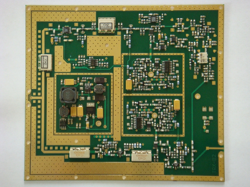
Three-layer-PCBS
Three-layer PCBs:
- basic core material: FR4, thickness 1/1.5mm, 18/18 µm copper
- Third layer printed: as polymer CU cream copper, galvanically strenghtened to 10 µm.
- Third layer laminated: CU-foil 18/or 35/µm laminated on a two-layer core 1 mm thick.
- To prevent a bow-effect, the pcb is produced actually as a 4-layer board
- drilled according to the drilling data, drilled holes metallized
- solder mask photolithographically placed
- service print
- galvanic tin
- tinned with Cn100C solder /not recommended/ or
- treated by OSP or
- galvanic gold over galvanic nickel
Maximum size:
- 250 x 300mm when galvanic tinned
- 250 x 300mm when HAL tinned /solder mask needed
- 250 x 300mm OSP
- 250 x 300mm galvanic gold
Needed documents:
- GERBER data with check prints or
- positive films of tracks, solder masks and service print. Set of data files allways required for production purposes.
- EXCELLON drill data
- The boards are milled to final dimension only. Others must be consulted during placing the order.
|


